
[ad_1]
Can superior semiconductors minimize emissions of greenhouse gases sufficient to make a distinction within the wrestle to halt local weather change? The reply is a convincing sure. Such a change is definitely properly underway.
Starting round 2001, the compound semiconductor gallium nitride fomented a revolution in lighting that has been, by some measures, the quickest expertise shift in human historical past. In simply 20 years, the share of the worldwide lighting market held by gallium-nitride-based light-emitting diodes has gone from zero to greater than 50 %, in line with a examine by the International Energy Agency. The analysis agency Mordor Intelligence just lately predicted that, worldwide, LED lighting might be accountable for slicing the electrical energy used for lighting by 30 to 40 % over the following seven years. Globally, lighting accounts for about
20 % of electrical energy use and 6 % of carbon dioxide emissions, in line with the United Nations Environment Program.
![]() Each wafer accommodates a whole lot of state-of-the-art energy transistorsPeter Adams
Each wafer accommodates a whole lot of state-of-the-art energy transistorsPeter Adams
This revolution is nowhere close to finished. Indeed, it’s about to leap to a better stage. The very semiconductor expertise that has remodeled the lighting trade, gallium nitride (GaN), can also be a part of a revolution in energy electronics that’s now gathering steam. It is one in every of two semiconductors—the opposite being silicon carbide (SiC)—which have begun displacing silicon-based electronics in huge and important classes of energy electronics.
GaN and SiC gadgets carry out higher and are extra environment friendly than the silicon parts they’re changing. There are numerous billions of those gadgets all around the world, and plenty of of them function for hours every single day, so the power financial savings are going to be substantial. The rise of GaN and SiC energy electronics will finally have a higher optimistic impression on the planet’s local weather than will the alternative of incandescent and different legacy lighting by GaN LEDs.
Virtually all over the place that alternating present have to be remodeled to direct present or vice versa, there might be fewer wasted watts. This conversion occurs in your cellphone’s or laptop computer’s wall charger, within the a lot bigger chargers and inverters that energy electrical automobiles, and elsewhere. And there might be related financial savings as different silicon strongholds fall to the brand new semiconductors, too. Wireless base-station amplifiers are among the many rising purposes for which these rising semiconductors are clearly superior. In the trouble to mitigate local weather change, eliminating waste in energy consumption is the low-hanging fruit, and these semiconductors are the way in which we’ll harvest it.
This is a brand new occasion of a well-recognized sample in expertise historical past: two competing improvements coming to fruition on the similar time. How will all of it shake out? In which purposes will SiC dominate, and through which will GaN prevail? A tough take a look at the relative strengths of those two semiconductors provides us some stable clues.
Why Power Conversion Matters in Climate Calculations
Before we get to the semiconductors themselves, let’s first take into account why we want them. To start with: Power conversion is all over the place. And it goes far past the little wall chargers that maintain our smartphones, tablets, laptops, and numerous different devices.
Power conversion is the method that adjustments electrical energy from the shape that’s accessible to the shape required for a product to carry out its operate. Some power is at all times misplaced in that conversion, and since a few of these merchandise run repeatedly, the power financial savings could be huge. Consider: Electricity consumption within the state of California remained basically flat from 1980 even because the financial output of the state skyrocketed. One of crucial explanation why the demand remained flat is that the effectivity of fridges and air conditioners elevated enormously over that interval. The single-greatest issue on this enchancment has been the usage of variable-speed drives primarily based on the insulated gate bipolar transistor (IGBT) and different energy electronics, which tremendously elevated effectivity.
SiC and GaN are going to allow far higher reductions in emissions. GaN-based applied sciences alone may result in a financial savings of over 1 billion tonnes of greenhouse gases in 2041 in simply the
United States and India, in line with an evaluation of publicly accessible information by Transphorm, a GaN-device firm I cofounded in 2007. The information got here from the International Energy Agency, Statista, and different sources. The similar evaluation signifies a 1,400-terawatt-hour power financial savings—or 10 to fifteen % of the projected power consumption by the 2 nations that 12 months.
Wide-Bandgap’s Advantages
Like an abnormal transistor, an influence transistor can act as an amplifying gadget or as a swap. An essential instance of the amplifying function is in wi-fi base stations, which amplify alerts for transmission to smartphones. All over the world, the semiconductor used to manufacture the transistors in these amplifiers is shifting from a silicon expertise referred to as laterally subtle metal-oxide semiconductor (LDMOS) to GaN. The newer expertise has many benefits, together with a power-efficiency enchancment of
10 % or extra relying on frequencies. In power-conversion purposes, then again, the transistor acts as a swap quite than as an amplifier. The customary approach is known as pulse-width modulation. In a standard kind of motor controller, for instance, pulses of direct-current electrical energy are fed to coils mounted on the motor’s rotor. These pulses arrange a magnetic discipline that interacts with that of the motor’s stator, which makes the rotor spin. The pace of this rotation is managed by altering the size of the pulses: A graph of those pulses is a sq. wave, and the longer the pulses are “on” quite than “off,” the extra rotational pace and torque the motor offers. Power transistors accomplish the on-and-off switching.
Pulse-width modulation can also be utilized in switching energy provides, probably the most widespread examples of energy conversion. Switching energy provides are the sort used to energy just about all private computer systems, cellular gadgets, and home equipment that run on DC. Basically, the enter AC voltage is transformed to DC, after which that DC is “chopped” right into a high-frequency alternating-current sq. wave. This chopping is completed by energy transistors, which create the sq. wave by switching the DC on and off. The sq. wave is utilized to a transformer that adjustments the amplitude of the wave to provide the specified output voltage. To get a gradual DC output, the voltage from the transformer is rectified and filtered.
The essential level right here is that the traits of the ability transistors decide, nearly solely, how properly the circuits can carry out pulse-width modulation—and due to this fact, how effectively the controller regulates the voltage. An splendid energy transistor would, when within the off state, utterly block present circulate even when the utilized voltage is excessive. This attribute is known as excessive electrical breakdown discipline power, and it signifies how a lot voltage the semiconductor is ready to stand up to. On the opposite hand, when it’s within the on state, this splendid transistor would have very low resistance to the circulate of present. This characteristic outcomes from very excessive mobility of the costs—electrons and holes—throughout the semiconductor’s crystalline lattice. Think of breakdown discipline power and cost mobility because the yin and yang of an influence semiconductor.
GaN transistors are very uncommon as a result of a lot of the present flowing by way of them is because of electron velocity quite than electron cost.
GaN and SiC come a lot nearer to this splendid than the silicon semiconductors they’re changing. First, take into account breakdown discipline power. Both GaN and SiC belong to a category referred to as wide-bandgap semiconductors. The bandgap of a semiconductor is outlined because the power, in electron volts, wanted for an electron within the semiconductor lattice to leap from the valence band to the conduction band. An electron within the valence band participates within the bonding of atoms throughout the crystal lattice, whereas within the conduction band electrons are free to maneuver round within the lattice and conduct electrical energy.
In a semiconductor with a large bandgap, the bonds between atoms are robust and so the fabric is normally in a position to stand up to comparatively excessive voltages earlier than the bonds break and the transistor is alleged to interrupt down. The bandgap of silicon is 1.12 electron volts, as in contrast with 3.40 eV for GaN. For the commonest kind of SiC, the band hole is 3.26 eV. [See table below, “The Wide-Bandgap Menagerie”]
Now let’s take a look at mobility, which is given in models of centimeters squared per volt second (cm2/V·s). The product of mobility and electrical discipline yields the speed of the electron, and the upper the speed the upper the present carried for a given quantity of shifting cost. For silicon this determine is 1,450; for SiC it’s round 950; and for GaN, about 2,000. GaN’s unusually excessive worth is the rationale why it may be used not solely in power-conversion purposes but additionally in microwave amplifiers. GaN transistors can amplify alerts with frequencies as excessive as 100 gigahertz—far above the three to 4 GHz usually considered the utmost for silicon LDMOS. For reference, 5G’s millimeter-wave frequencies high out at 52.6 GHz. This highest 5G band will not be but broadly used, nevertheless, frequencies as much as 75 GHz are being deployed in dish-to-dish communications, and researchers at the moment are working with frequencies as excessive as 140 GHz for in-room communications. The urge for food for bandwidth is insatiable.
These efficiency figures are essential, however they’re not the one standards by which GaN and SiC must be in contrast for any explicit software. Other vital elements embody ease of use and price, for each the gadgets and the programs into which they’re built-in. Taken collectively, these elements clarify the place and why every of those semiconductors has begun displacing silicon—and the way their future competitors might shake out.
SiC Leads GaN in Power Conversion Today…
The first commercially viable SiC transistor that was superior to silicon was launched by Cree (now Wolfspeed) in 2011. It may block 1,200 volts and had a respectably low resistance of 80 milliohms when conducting present. Today there are three completely different sorts of SiC transistors in the marketplace. There’s a trench MOSFET (metal-oxide semiconductor field-effect transistor) from Rohm; DMOSs (double-diffused MOSs) from Infineon Technologies, ON Semiconductor Corp., STMicroelectronics, Wolfspeed, and others; and a vertical-junction field-effect transistor from Qorvo.
One of the massive benefits of SiC MOSFETs is their similarity to conventional silicon ones—even the packaging is equivalent. A SiC MOSFET operates in basically the identical approach as an abnormal silicon MOSFET. There’s a supply, a gate, and a drain. When the gadget is on, electrons circulate from a closely doped
n-type supply throughout a calmly doped bulk area earlier than being “drained” by way of a conductive substrate. This similarity implies that there’s little studying curve for engineers making the swap to SiC.
Compared to GaN, SiC has different benefits. SiC MOSFETs are inherently “fail-open” gadgets, that means that if the management circuit fails for any motive the transistor stops conducting present. This is a vital characteristic, as a result of this attribute largely eliminates the chance {that a} failure may result in a brief circuit and a hearth or explosion. (The worth paid for this characteristic, nevertheless, is a decrease electron mobility, which will increase resistance when the gadget is on.)
…But GaN Is Gaining
GaN brings its personal distinctive benefits. The semiconductor first established itself commercially in 2000 within the markets for light-emitting diodes and semiconductor lasers. It was the primary semiconductor able to reliably emitting shiny inexperienced, blue, purple, and ultraviolet mild. But lengthy earlier than this business breakthrough in optoelectronics, I and different researchers had already demonstrated the promise of GaN for high-power electronics. GaN LEDs caught on shortly as a result of they crammed a void for environment friendly lighting. But GaN for electronics needed to show itself superior to current applied sciences: particularly, silicon CoolMOS transistors from Infineon for energy electronics, and silicon-LDMOS and gallium-arsenide transistors for radio-frequency electronics.
GaN’s predominant benefit is its extraordinarily excessive electron mobility. Electric present, the circulate of cost, equals the focus of the costs multiplied by their velocity. So you may get excessive present due to excessive focus or excessive velocity or some mixture of the 2. The GaN transistor is uncommon as a result of a lot of the present flowing by way of the gadget is because of electron velocity quite than cost focus. What this implies in follow is that, compared with Si or SiC, much less cost has to circulate into the gadget to modify it on or off. That, in flip, reduces the power wanted for every switching cycle and contributes to excessive effectivity.
Meanwhile, GaN’s excessive electron mobility permits switching speeds on the order of fifty volts per nanosecond. That attribute means energy converters primarily based on GaN transistors function effectively at frequencies within the a number of a whole lot of kilohertz, versus about 100 kilohertz for silicon or SiC.
Taken collectively, the excessive effectivity and excessive frequency allows the ability converter primarily based on GaN gadgets to be fairly small and light-weight: High effectivity means smaller warmth sinks, and operation at excessive frequencies implies that the inductors and capacitors could be very small, too.
One drawback of GaN semiconductors is that they don’t but have a dependable insulator expertise. This complicates the design of gadgets which can be fail-safe—in different phrases, that fail open if the management circuit fails.
There are two choices to realize this usually off attribute. One is to equip the transistor with a kind of gate that removes the cost within the channel when there’s no voltage utilized to the gate and that conducts present solely on software of a optimistic voltage to that gate. These are referred to as enhancement-mode gadgets. They are supplied by
EPC, GaN Systems, Infineon,Innoscience, and Navitas, for instance. [See illustration, “Enhancement–ModeGaNTransistor“]
The different possibility is known as the cascode resolution. It makes use of a separate, low-loss silicon field-effect transistor to supply the fail-safe characteristic for the GaN transistor. This cascode resolution is utilized by
Power Integrations, Texas Instruments, and Transphorm. [See illustration, “Cascoded Depletion-Mode GaN Transistor”]
No comparability of semiconductors is full with out a consideration of prices. A tough rule of thumb is—smaller die dimension means decrease price. Die dimension is the bodily space of the built-in circuit containing the gadgets.
SiC gadgets now usually have smaller dies than GaN ones. However, SiC’s substrate and fabrication prices are increased than these for GaN and, generally, the ultimate gadget prices for purposes at 5 kilowatts and better should not a lot completely different at the moment. Future developments, although, are more likely to favor GaN. I base this perception on the relative simplicity of GaN gadgets, which is able to imply manufacturing prices low sufficient to beat the bigger die dimension.
That stated, for GaN to be viable for a lot of high-power purposes that additionally demand excessive voltages, it will need to have an economical, high-performance gadget rated for 1,200 V. After all, there are already SiC transistors accessible at that voltage. Currently, the closest commercially accessible GaN transistors are rated for 900 V, produced by Transphorm, which I cofounded with
Primit Parikh. Lately, we have now additionally demonstrated 1,200-V gadgets, fabricated on sapphire substrates, which have each electrical and thermal efficiency on a par with SiC gadgets.
Projections from the analysis agency Omdia for 1,200-V SiC MOSFETs point out a worth of 16 cents per ampere in 2025. In my estimation, due to the decrease price of GaN substrates, the worth of first-generation 1,200-V GaN transistors in 2025 might be lower than that of their SiC counterparts. Of course, that’s simply my opinion; we’ll all know for positive how this may shake out in a few years.
GaN vs. SiC: Handicapping the Contests
With these relative benefits and downsides in thoughts, let’s take into account particular person purposes, one after the other, and shed some mild on how issues may develop.
•
Electric automobile inverters and converters: Tesla’s adoption of SiC in 2017 for the onboard, or traction, inverters for its Model 3 was an early and main win for the semiconductor. In an EV, the traction inverter converts the DC from the batteries to AC for the motor. The inverter additionally controls the pace of the motor by various the frequency of the alternating present. Today, Mercedes-Benz and Lucid Motors are additionally utilizing SiC of their inverters and different EV makers are planning to make use of SiC in upcoming fashions, in line with information reviews. The SiC gadgets are being provided by Infineon, OnSemi, Rohm, Wolfspeed, and others. EV traction inverters sometimes vary from about 35 kW to 100 kW for a small EV to about 400 kW for a big automobile.
However, it’s too quickly to name this contest for SiC. As I famous, to make inroads on this market, GaN suppliers must supply a 1,200-V gadget. EV electrical programs now sometimes function at simply 400 volts, however the Porsche Taycan has an 800-V system, as do EVs from Audi, Hyundai, and Kia. Other automakers are anticipated to comply with their lead in coming years. (The Lucid Air has a 900-V system.) I anticipate to see the primary business 1,200-V GaN transistors in 2025. These gadgets might be used not solely in automobiles but additionally in high-speed public EV chargers.
The increased switching speeds attainable with GaN might be a robust benefit in EV inverters, as a result of these switches make use of what are referred to as hard-switched methods. Here, the way in which to boost efficiency is to modify very quick from on to off to reduce the time when the gadget is each holding excessive voltage
and passing excessive present.
Besides an inverter, an EV additionally sometimes has an
onboard charger, which allows the automobile to be charged from wall (mains) present by changing AC to DC. Here, once more, GaN could be very enticing, for a similar causes that make it a good selection for inverters.
•
Electric-grid purposes: Very-high-voltage energy conversion for gadgets rated at 3 kV and better will stay the area of SiC for at the least the following decade. These purposes embody programs to assist stabilize the grid, convert AC to DC and again once more at transmission-level voltages, and different makes use of.
•
Phone, pill, and laptop computer chargers: Starting in 2019, GaN-based wall chargers turned accessible commercially from corporations akin to GaN Systems, Innoscience, Navitas, Power Integrations, and Transphorm. The excessive switching speeds of GaN coupled with its usually decrease prices have made it the incumbent in lower-power markets (25 to 500 W), the place these elements, together with small dimension and a sturdy provide chain, are paramount. These early GaN energy converters had switching frequencies as excessive as 300 kHz and efficiencies above 92 %. They set information for energy density, with figures as excessive as 30 W per cubic inch (1.83 W/cm3)—roughly double the density of the silicon-based chargers they’re changing.
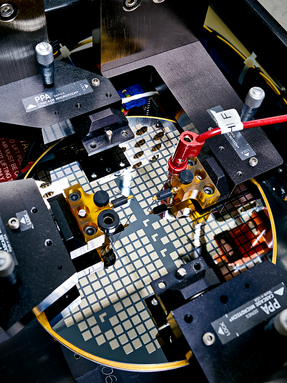 An automated system of probes applies a excessive voltage to emphasize take a look at energy transistors on a wafer. The automated system, at Transphorm, exams every one in every of some 500 die in minutes. Peter Adams
•
Solar-power microinverters: Solar-power technology has taken off lately, in each grid-scale and distributed (family) purposes. For each set up, an inverter is required to transform the DC from the photo voltaic panels to AC to energy a house or launch the electrical energy to the grid. Today, grid-scale photovoltaic inverters are the area of silicon IGBTs and SiC MOSFETs. But GaN will start making inroads within the distributed photo voltaic market, notably.
Traditionally, in these distributed installations, there was a single inverter field for the entire photo voltaic panels. But more and more installers are favoring programs in which there’s a separate microinverter for every panel, and the AC is mixed earlier than powering the home or feeding the grid. Such a setup means the system can monitor the operation of every panel with a purpose to optimize the efficiency of the entire array.
Microinverter or conventional inverter programs are vital to the fashionable information middle. Coupled with batteries they create an
uninterruptible energy provide to forestall outages. Also, all information facilities use power-factor correction circuits, which regulate the ability provide’s alternating-current waveforms to enhance effectivity and take away traits that might harm tools. And for these, GaN offers a low-loss and economical resolution that’s slowly displacing silicon.
•
5G and 6G base stations: GaN’s superior pace and excessive energy density will allow it to win and finally dominate purposes within the microwave regimes, notably 5G and 6G wi-fi, and business and navy radar. The predominant competitors listed below are arrays of silicon LDMOS gadgets, that are cheaper however have decrease efficiency. Indeed, GaN has no actual competitor at frequencies of 4 GHz and above.
For 5G and 6G wi-fi, the vital parameter is bandwidth, as a result of it determines how a lot data the {hardware} can transmit effectively. Next-generation 5G programs may have practically 1 GHz of bandwidth, enabling blazingly quick video and different purposes.
Microwave-communication programs that use silicon-on-insulator applied sciences present a 5G+ resolution utilizing high-frequency silicon gadgets the place every gadget’s low output energy is overcome with giant arrays of them. GaN and silicon will coexist for some time on this area. The winner in a particular software might be decided by a trade-off amongst system structure, price, and efficiency.
•
Radar: The U.S. navy is deploying many ground-based radar programs primarily based on GaN electronics. These embody the Ground/Air Task Oriented Radar and the Active Electronically Scanned Array Radar constructed by Northrup-Grumman for the U.S. Marine Corps. Raytheon’s SPY6 radar was delivered to the U.S. Navy and examined for the primary time at sea in December 2022. The system tremendously extends the vary and sensitivity of shipborne radar.
The Wide-Bandgap Battle Is Just Beginning
Today, SiC dominates in EV inverters, and usually wherever voltage-blocking functionality and energy dealing with are paramount and the place the frequency is low. GaN is the popular expertise the place high-frequency efficiency issues, akin to in base stations for 5G and 6G, and for radar and high-frequency power-conversion purposes akin to wall-plug adapters, microinverters, and energy provides.
But the tug-of-war between GaN and SiC is simply starting. Regardless of how the competitors performs out, software by software and market by market, we are able to say for positive that the Earth’s atmosphere might be a winner. Countless billions of tonnes of greenhouse gases might be prevented in coming years as this new cycle of technological alternative and rejuvenation wends its approach inexorably ahead.
From Your Site Articles
Related Articles Around the Web
[ad_2]