
[ad_1]
Interconnects—these typically nanometers-wide steel wires that hyperlink transistors into circuits on an IC—are in want of a serious overhaul. And as chip fabs march towards the outer reaches of Moore’s Law, interconnects are additionally changing into the trade’s choke level.
“For some 20-25 years now, copper has been the metal of choice for interconnects. However we’re reaching a point where the scaling of copper is slowing down,” IBM’s Chris Penny, advised engineers final month on the IEEE International Electron Device Meeting (IEDM). “And there is an opportunity for alternative conductors.”
Ruthenium is a number one candidate, but it surely’s not so simple as swapping one steel for one more, in line with analysis reported at IEDM 2022. The processes of how they’re fashioned on a chip should be turned the other way up. These new interconnects will want a special form and the next density. These new interconnects can even want higher insulation, lest signal-sapping capacitance take away all their benefit.
Even the place the interconnects go is ready to alter, and shortly. But research are beginning to present, the good points from that shift include a sure value.
Ruthenium, high vias, and air gaps
Among the replacements for copper, ruthenium has gained a following. But analysis is exhibiting that the outdated formulation used to construct copper interconnects are an obstacle to ruthenium. Copper interconnects are constructed utilizing what’s known as a damascene course of. First chip makers use lithography to carve the form of the interconnect into the dielectric insulation above the transistors. Then they deposit a liner and a barrier materials, which prevents copper atoms from drifting out into the remainder of the chip to muck issues up. Copper then fills the ditch. In truth, it overfills it, so the surplus should be polished away.
All that further stuff, the liner and barrier, take up house, as a lot as 40-50 % of the interconnect quantity, Penny advised engineers at IEDM. So the conductive a part of the interconnects are narrowing, particularly within the ultrafine vertical connections between layers of interconnects, rising resistance. But IBM and Samsung researchers have discovered a option to construct tightly-spaced, low-resistance ruthenium interconnects that don’t want a liner or a seed. The course of known as spacer assisted litho-etch litho-etch, or SALELE, and, because the identify implies, it depends on a double serving to of extreme-ultraviolet lithography. Instead of filling in trenches, it etches the ruthenium interconnects out of a layer or steel after which fills within the gaps with dielectric.
The researchers obtain the perfect resistance utilizing tall, skinny horizontal interconnects. However, that will increase capacitance, buying and selling away the profit. Fortunately, as a result of manner SALELE builds vertical connections known as vias—on high of horizontal interconnects as an alternative of beneath them—the areas between slender ruthenium traces can simply be full of air, which is the perfect insulator accessible. For these tall, slim interconnects “the potential benefit of adding an air gap is huge… as much as a 30 percent line capacitance reduction,” mentioned Penny.
The SALELE course of “provides a roadmap to 1-nanometer processes and beyond,” he mentioned.
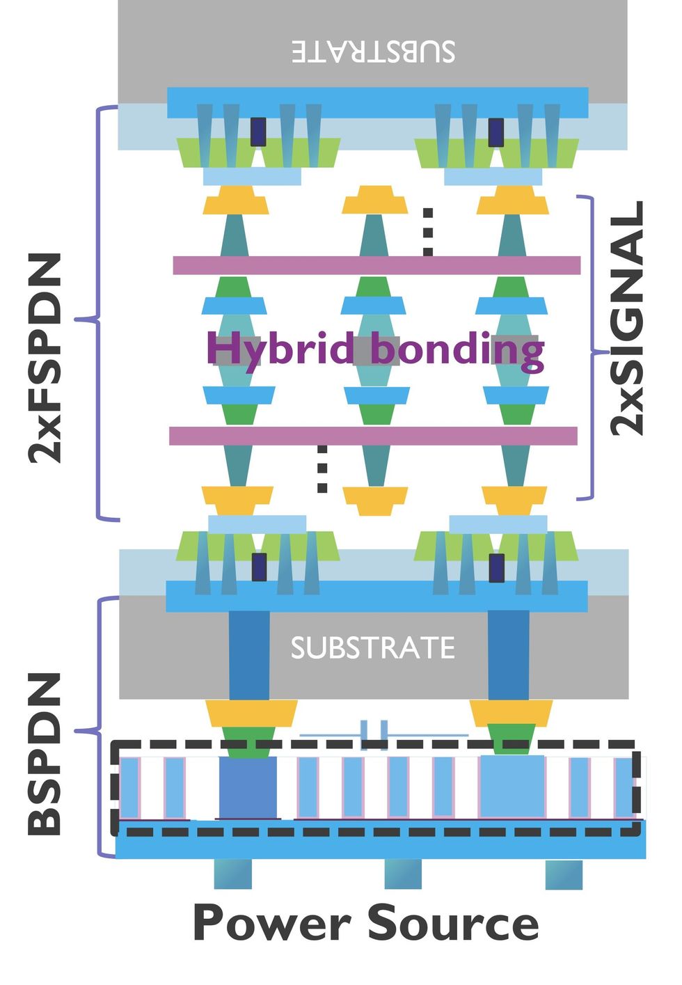
Buried rails, back-side energy supply, and sizzling 3D chips
As early as 2024, Intel plans to make a radical change to the placement of interconnects that carry energy to transistors on a chip. The scheme, known as back-side energy supply, takes the community of energy supply interconnects and strikes it beneath the silicon, in order that they method the transistors from beneath. This has two major benefits: It permits electrical energy to stream by wider, much less resistive interconnects, resulting in much less energy loss. And it frees up room above the transistors for signal-carrying interconnects, that means logic cells may be smaller. (Researchers from Arm and the Belgian nanotech analysis hub Imec defined all of it right here.)
At IEDM 2022, Imec researchers got here up with some formulation to make back-side energy work higher, by discovering methods to maneuver the top factors of the facility supply community, known as buried energy rails, nearer to transistors with out messing up these transistors’ digital properties. But additionally they uncovered a considerably troubling downside, back-side energy might result in a build-up of warmth when utilized in 3D stacked chips.
First the excellent news: When imec researchers explored how a lot horizontal distance you want between a buried energy rail and a transistor, the reply was just about zero. It took some further cycles of processing to make sure that the transistors have been unaffected, however they confirmed that you would be able to construct the rail proper beside the transistor channel area—although nonetheless tens of nanometers beneath it. And that might imply even smaller logic cells.
Now the dangerous information: In separate analysis, imec engineers simulated a number of variations of the identical future CPU. Some had the form of energy supply community in use at present, known as front-side energy supply, the place all interconnects, each information and energy, are in-built layers above the silicon. Some had back-side energy supply networks . And one was a 3D stack of two CPUs, the underside having back-side energy and the highest having front-side.
Back-side energy’s benefits have been confirmed by the simulations of the 2D CPUs. Compared to front-side supply, it reduce the loss from energy supply in half, for instance. And transient voltage drops have been much less pronounced. What’s extra, the CPU space was 8 % smaller. However, the most popular a part of back-side chip was about 45 % hotter than the most popular a part of a front-side chip. The possible trigger is that back-side energy requires thinning the chip right down to the purpose the place it must be bonded to a separate piece of silicon simply to stay secure. That bond acts as a barrier to the stream of warmth.
 Researchers examined a state of affairs the place a CPU [bottom grey] with a back-side energy supply community is bonded to a second CPU having a front-side energy supply community [top grey].
The actual issues arose with the 3D IC. The high CPU has to get its energy from the underside CPU, however the lengthy journey to the highest had penalties. While the underside CPU nonetheless had higher voltage-drop traits than a front-side chip, the highest CPU carried out a lot worse in that respect. And the 3D IC’s energy community ate up greater than twice the facility {that a} single front-side chip’s community would devour. Worse nonetheless, warmth couldn’t escape the 3D stack very nicely, with the most popular a part of the underside die virtually 2.5 occasions as sizzling as a single front-side CPU. The high CPU was cooler, however not by a lot.
The 3D IC simulation is admittedly considerably unrealistic, imec’s Rongmei Chen advised engineers at IEDM. Stacking two in any other case an identical CPUs atop one another is an unlikely state of affairs. (It’s rather more widespread to stack reminiscence with a CPU.) “It’s not a very fair comparison,” he mentioned. But it does level out some potential points.
From Your Site Articles
Related Articles Around the Web
[ad_2]